
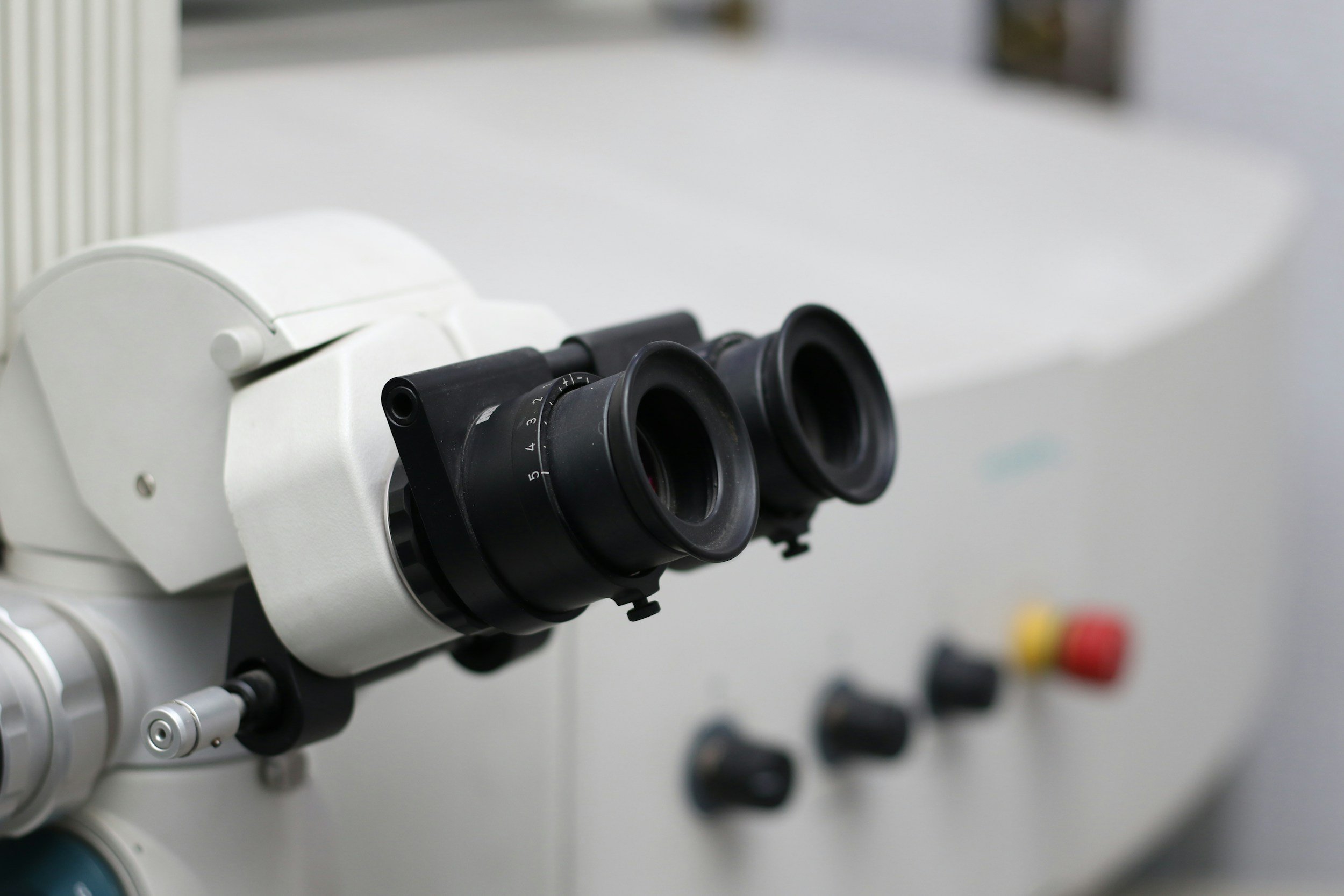
Hitachi’s Holography Electron Microscope achieves unprecedented atomic-scale resolution
A team of researchers from Japan, including scientists from Hitachi, has achieved a groundbreaking resolution of 0.47 nm using holography electron microscopy to visualise magnetic fields at the atomic scale.
The advancement made possible through new image acquisition techniques and defocusing correction algorithms marks a significant step forward in materials science and various applied fields.
Electron holography microscopy is a sophisticated technique for visualising magnetic fields in materials at atomic resolution. A collaborative research team from Hitachi, Kyushu University, RIKEN, and HREM Research Inc., in conjunction with the National Institute of Advanced Industrial Science and Technology (AIST) and the National Institute for Materials Science (NIMS), has pushed the boundaries of this technology. When imaging magnetic atomic lattices in a crystal, they achieved an unprecedented resolution of 0.47 nm.
High-performance materials with tailored characteristics are crucial in numerous technological advancements in electronics, catalysis, transportation, and energy generation. The arrangement of atoms and electron behaviour within these materials dictate their properties.
The magnetic fields at the interfaces between different materials or atomic layers are vital in explaining various physical phenomena. Before this advancement, the highest resolution for observing such magnetic fields was 0.67 nm, achieved by Hitachi in 2017.
The research team overcame significant limitations of existing holography electron microscopes. They developed an automated system to control and tune the device during data acquisition, allowing the rapid collection of 10,000 images over 8.5 hours. Through specific averaging operations, they minimised noise, resulting in clearer images with distinct electric and magnetic field data.
A key challenge was correcting minute defocusing, which caused image aberrations.
“The idea of post-image-capture correction of aberrations we employed is exactly the same as that which had motivated Dr. Dennis Gabor to invent electron holography in 1948. In other words, the methodology was already theoretically established.
“Until now, however, there had been no technological implementations for such automated correction in off-axis electron holography,” explained Chief Researcher Toshiaki Tanigaki from Hitachi.
The approach enabled defocusing correction due to minor focus shifts, producing images free of residual aberrations and revealing atomic positions and phases.
Utilising these innovations, the team conducted electron holography measurements on samples of Ba2FeMoO6, a layered crystalline material with distinct magnetic fields in adjacent atomic layers. Their experimental results, confirmed through simulations, set a new record by achieving a resolution of 0.47 nm.
“This result opens doors to direct observations of the magnetic lattices in specific areas, such as interfaces and grain boundaries, in many materials and devices,” commented Tanigaki.
“Our study marks the first step towards investigating many veiled phenomena whose existence can be revealed by electron spin configurations in magnetic materials.”
“Our atomic-resolution holography electron microscope will be used by various parties, contributing to advances in a wide range of fields ranging from fundamental physics to next-generation devices. Ultimately, this would pave the way for the realisation of a carbon-neutral society through the development of high-performance magnets and highly functional materials that are essential for decarbonisation and energy-saving efforts,” concluded Tanigaki, looking towards future possibilities.